Tips for Electronic Printed circuit Board Design
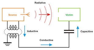
EMI/EMC problems may be approached at the component, PC board or
enclosure levels. However, it is much more
efficient to deal with these problems as close to the source or susceptible
victim as possible. Therefore, it is
important to consider these tips as guidelines for PCB design and layout so that
problems may be identified and prevented prior to actual fabrication of the
equipment.
(1) EMI controls should be applied at the circuit and box levels
prior to addressing EMI at the interconnected and system levels.
(2) Digital circuits are more likely to be the source of emissions
due to the handling of periodic waveforms and the fast clock/switching
rates. Analog circuits are more
likely to be the susceptible victims due to higher gain functions.
(3) The source or susceptible victim of most EMI problems is
typically an electronic component. Although active components are usually the sources of EMI, passive
components often contribute to it, depending on the signal frequencies and
component's characteristics. For example, an inductor can become
predominantly capacitive due to the high frequency parasitic coupling between
windings. A capacitor can develop
parasitic series inductance due to its internal inductance and external lead
inductance at high fundamental and harmonic frequencies.
(4) EMI problems involving an active component can be the result
of the device's output transferring the emissions or its input providing the
path for susceptibility. However, at high frequencies the active component may become a
direct radiator or receptor of EMI. Also, the component’s power and ground connections can provide
paths for both emissions and susceptibility.
(5) Although common mode currents are usually small compared to
differential mode currents, they can be the main cause of radiated emissions.
(6) Emissions and susceptibility that are typical in single layer,
free wired (using power and ground traces instead of planes) PC Board design,
can be greatly improved by using multi-layer PC boards with power planes. High capacitance between a forward signal and
its return path (ground plane) provides containment of the electric
field. Low inductance of the paths provides for magnetic flux
cancellation. Although not always
realistic in a PCB stack-up design, a trace should be spaced one dielectric layer
away from its associated return path and the voltage and ground planes should
be as closely spaced as possible.
(7) PCB stack-up design is important in containing the
electromagnetic fields, while providing for additional bypassing and decoupling
of the power bus and minimizing bus voltage transients. Some of the benefits of multi-layer PC board
design with power planes are:
a. The power planes, if properly designed, will provide an image
plane effect. Since the return
currents in the power planes are equal and opposite polarity to the associated
signal currents, their electromagnetic fields will tend to cancel. Power planes can also reduce the loop areas of
signal and power traces, resulting in a decrease of EMI emissions and
susceptibility.
b. A ground plane can lower the overall ground
impedance, thus reducing high frequency ground bounce. Also, the impedance between the ground and
voltage planes is lowered at the high frequencies and this reduces power bus
ringing.
(8) Clocked IC’s with rapid output transitions can be very
demanding on voltage and current distribution components such as the power
supply, power bus, and power planes. The inductance of the power bus can prevent the rapid energy
transfer needed to meet the quick output transitions and fast rise times. This can be improved with the placement of
decoupling capacitors at the IC’s power pins. The capacitors must be properly selected in
their frequency response to deliver the energy needed at the IC’s output
frequency spectrum. However, as the number
of decoupling paths increase, so do the number of voltage drops across them and
this can result in power bus transients along with the associated common mode
emissions. This problem can be
minimized with proper power plane design in the area of the IC’s. The power plane acts as an effective high
frequency capacitor, and consequently, as an additional energy source needed
for cleaner IC outputs.
Happy Reading
Ruby


Comments
Post a Comment