Strategies for Laying Out Printed Circuit Boards.
Most board designers employ a list of
guidelines to help place components and route traces. For example, a typical
guideline might be "minimize the length of all traces carrying a digital
clock signal." Often, a designer is not familiar with the reason for the
guideline or does not fully understand the consequences of violating the
guideline for a particular application.
Quiz Question
Suppose you're laying
out a high-speed multi-layer printed circuit board and you need to route a
trace carrying a high-frequency signal from a digital component to an analog
amplifier. You want to minimize the chance of having an electromagnetic
compatibility (EMC) problem, so you search the web for EMC design guidelines
and you find three guidelines that seem to pertain to your situation:
1.
minimize the length of
high-speed traces;
2.
always gap
any solid planes between analog and digital circuits; and
3.
never let a
high-speed trace cross over a gap in the signal return plane.
You envision the three
possible routing strategies illustrated in Figure 2. The first routing strategy
routes the trace directly between the two components, but leaves the plane
between them solid. The second routing strategy gaps the plane, but routes the
trace over the gap. The third routing strategy routes the trace around the gap.
Each of these alternatives violates one of the guidelines. Which is the best
choice?
Figure 2: Which is the best trace routing alternative?
Is each alternative equally good because it
satisfies 2 of 3 guidelines? Are they all bad because they all violate at least
one guideline? These are the types of questions that circuit board designers
are faced with every day. Making the right choice can be the difference between
a board that meets all requirements and a board that has severe radiated
emissions or susceptibility problems. In this case, one of the choices is much
better than the other two. However before we reveal the correct answer, let's
develop a strategy for evaluating printed circuit board layouts. With a proper
strategy, the correct answer to this quiz question should become apparent.
4 steps that
every EMC engineer should apply when laying out a printed circuit board or reviewing
an existing board design. These steps are:
·
Identify potential EMI
sources and victims
·
Identify critical
current paths
·
Identify potential
antenna parts
·
Explore possible
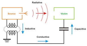
coupling mechanisms.
By taking the steps outlined above first,
component placement and trace routing decisions will become clearer. It should
also be much more apparent which design guidelines are most important and which
are not important at all for a specific design.
In my next article i will discuss all the points one by one mentioned above.
Thanks for reading..
Ruby


Comments
Post a Comment