Difference Between Plated through Hole and Non Plated Through Hole
During PCB design many issues come across and one of them is in the regard of non-plated and plated through holes. What is the difference between them and where should one use which one? is a commonly asked question. Here we will briefly discuss this issue.
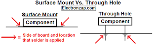
Through hole components have leads(straight or clinched) and these leads are put through holes available or made on the PCB insulating materials and soldered on the other side onto the copper tracks.
The difference between non plated through hole and plated through hole is the presence of plated copper inside the insulating base material as shown in the pictures below. The presence of this plated through hole has in turn effect on electrical properties and mechanical stability. When component leads is soldered through plated holes then (1)the electrical resistance by the joint formed becomes less and (2) the mechanical stability increases. This is not the case with the non plated holes and hence plated through holes are more beneficial than non plated through hole joints.
Other differences include the cost and area. Plated through holes PCB is more costly than the non-plated through hole PCB. And plated through holes PCB consumes less space/area than the non-plated through hole PCB.
The advantage of using non plated through holes come from simpler and maybe quicker manufacturing.
The figure below shows the non plated through hole and plated through hole where straight leads of component is used.
Thanks,
Through hole components have leads(straight or clinched) and these leads are put through holes available or made on the PCB insulating materials and soldered on the other side onto the copper tracks.
The difference between non plated through hole and plated through hole is the presence of plated copper inside the insulating base material as shown in the pictures below. The presence of this plated through hole has in turn effect on electrical properties and mechanical stability. When component leads is soldered through plated holes then (1)the electrical resistance by the joint formed becomes less and (2) the mechanical stability increases. This is not the case with the non plated holes and hence plated through holes are more beneficial than non plated through hole joints.
Other differences include the cost and area. Plated through holes PCB is more costly than the non-plated through hole PCB. And plated through holes PCB consumes less space/area than the non-plated through hole PCB.
The advantage of using non plated through holes come from simpler and maybe quicker manufacturing.
The figure below shows the non plated through hole and plated through hole where straight leads of component is used.
 |
| Fig 1: Non-plated through hole with straight lead |
 |
| Fig 2: Plated through hole with straight lead |
Ruby


Comments
Post a Comment