EMC design considerations

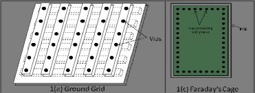
Any electronic product consists of various modules, where each module has to communicate with the other for its operation or to report the status. With the ever-growing demand for faster processing speeds, better response time and more throughputs, always narrow down to highspeed circuits. If not contained properly, the signal flowing t h r o u g h these circuits may radiate energy and can cause problems in the operation of devices in the near vicinity. Now, engineers must consider not only the actual logic on the PCB, but also several other aspects that affect the circuit, including power consumption, PCB size, environment noise, andEMC. The following 10 key EMC design considerations can serve as guidelines and describe how hardware engineers can address EMC issues during the PCB design phase for a system free of EMC faults: 1. Ground Planes : A low-inductance ground system is the most vital element when designing a PCB for minimizing EMI. Maximizing the ground area on a PCB re...