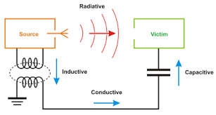
placement of connectors and groundings to reduce EMI
Cables and Connectors
(1) Cables should be grouped according to their function such as
power, analog, digital, and RF.
(2) Separate connector assemblies should be used for analog and
digital signals.
(3) Analog and digital connectors should be located as far apart
as possible.
(4) Analog and digital signal pins should be separated by unused
grounded pins when sharing the same I/O connector.
(5) Individual pins should be used inside the I/O connector for
each signal return so that all return circuits remain separated.
(6) Connector crosstalk may be reduced by using separate power and
ground pins for each signal and by reducing the circuit’s loading and current
flow.
(7) Cable shields should be grounded to equipment housing at the
I/O points.
(8) Shielded I/O cables are most effective if grounded at both
ends.
(9) Cable common mode currents should be removed at the
equipment’s metal housing prior to internal connections.
(10) Cables should be routed close to ground planes, shielded
structures, and cable trays.
Grounding
(1) Use ground planes instead of vectorial traces.
(2) Ground traces should be as short and thick as possible.
(3) Decouple signal and RF circuit grounds.
PCB Layout
(1) Use multi-layer PC
boards rather than single-layer boards whenever possible.
(2) If a single layer board must be used, a ground plane should be
utilized to help reduce radiation.
(3) Top and bottom ground planes can help reduce radiation from
multi-layer boards by at least 10 dB.
(4) Segmented PC board ground planes are useful for reducing cable
radiation due to common mode currents.
(5) Power and return planes should be located on opposite sides of
a multi-layer PCB. Effective power planes
are low in inductance. Therefore, any
transients that may develop on the power planes will be at lower levels,
resulting in lower common mode EMI.
(6) Connection of the power
planes to high frequency IC power pins should be as close to the IC pins as
possible. Faster rise times may require connections directly to the pads
of the IC power pins.
(7) Analog and digital circuits are susceptible to interaction
when located in close proximity to each other. These should be located on different layers of
the PC board whenever possible. If the circuits must be located on the same layer, they should be
separated into analog and digital areas with proper isolation layout.
(8) High frequency traces, such as those used for clock and
oscillator circuits, should be contained by two ground planes. This provides for maximum isolation. The reactance of a trace or conductor can easily
exceed its dc resistance as frequency increases. If this trace is run close to its ground plane,
the inductance can be reduced by about one third.
(9) Additional EMI preventive measures for clock/oscillator traces
include the utilization of guard traces grounded to the ground plane at several
locations. The shielding of clock and oscillator components with foil or small
metallic enclosures may also be needed.
(10) Overall circuit cross-talk increases by a factor of two
whenever the clock rate is doubled. EMI radiation and cross-talk may be reduced by minimizing the PC
board trace height above the ground plane.
(11) PC board edge radiation may be the result of traces being
located too close to the board edge. This can be minimized by keeping traces at a distance of at least
3 times the board thickness away from the board edge.
(12) PC board trace stacking should be avoided if possible. Otherwise, it should be limited to one trace
height in order to reduce radiation, cross-talk and impedance mismatches.
(13) Parallel traces are often susceptible to cross-talk. These should be separated by at least 2 trace
widths for cross-talk reduction.
Thanks,
Ruby


Comments
Post a Comment