Posts

Showing posts from 2016

PCB footprint creation using PADS

Image

When are differential pairs needed?

There are three reasons to use differential pairs in a digital or analog signal path. Where the ground connections between the ends of the signal path are poor. The most important one is that the ground connection between the two ends of the signal path can be  very poor and data quality will not be compromised.Compare this to a single-ended signal path such as LVCMOS, where the signal arriving at the receiver is compared to a reference level in the receiver. If the grounds between the two ends are offset, the logic levels will be offset and one or the other of the two logic levels is compromised. This ability to “ignore” ground offsets has been the backbone of the wired Internet from the onset. In the case of Ethernet,the two ends of these links are transformer coupled. Where there is significant attenuation along the signal path. A second reason to use differential signaling is that the link can suffer substantial attenuation  of the signal and still function prop

What is a differential pair and how does it work?

Image
In its most basic form, a differential pair is made up of two transmission lines that have  equal and opposite polarity signals travelling on them. The property that these two signals  have in common is that they are equal and opposite and they are tightly timed to each other. Beyond these two characteristics there are no other properties that matter when a design uses  differential pairs. Maintaining the equal and opposite amplitude and timing relationship is the  guiding concept when using differential pairs.                       figure 1 Figure 1 is a typical CMOS differential pair driver and receiver pair. It is the usual circuit  used in LVDS (low voltage differential signaling) type signaling protocols.                                figure 2 As can be seen from Figure 1, there are two independent transmission lines of characteristic  impedance, Z0, connecting the drivers and receivers. Each of these is terminated with a parallel  termination of va

Printed circcuit board basic description video

Image

Overview of Capacitor technology

Image
Capacitors (and inductors) have the ability to store electrical energy, inductors store energy as a magnetic field around the component, but the capacitor stores electrical energy directly, as an ELECTROSTATIC FIELD created between two metal "plates". Basic Circuit symbols for capacitors • High Voltage Electrolytic- used in power supplies.  • Axial Electrolytic; lower voltage smaller size for general purpose where large capacitance values are needed.  • High Voltage disk ceramic; small size and capacitance value, excellent tolerance characteristics.  • Metalised Polypropylene; small size for values up to around 2µF good reliability.  • Sub miniature Multi layer ceramic chip (surface mount) capacitor. Relatively high         capacitance for size achieved by multiple layers, effectively several capacitors in parallel.  Uses of Capacitors. Decoupling --The most prevalent use of capacitors is to decouple a system,such as in

PCB description

Pcb

Interactive Placement and routing stratagies

Image
PCB layout is a means to combine your artistic side and your creative skills with the power of automation. I always say that if a PCB design looks good, it will probably work well. However, neatness in routing often leads to unwanted crosstalk as trace segments are routed in parallel for long distances. Interactive Placement  - To obtain a high route-completion rate, component placement is extremely important. If the board is difficult to route, it may just be the result of poor placement, slots/gates positioned all over the board, or perhaps the sequence of pins on components are flipped. We need to help the router as much as possible by opening route channels and providing space for vias.  Interactive placement is best done by cross-probing and dragging the components one-by-one from the schematic to place on the PCB—taking functionality and design constraints into account.  During placement, consideration should not only be given to routing, but also to inspection

EMC design considerations

Image
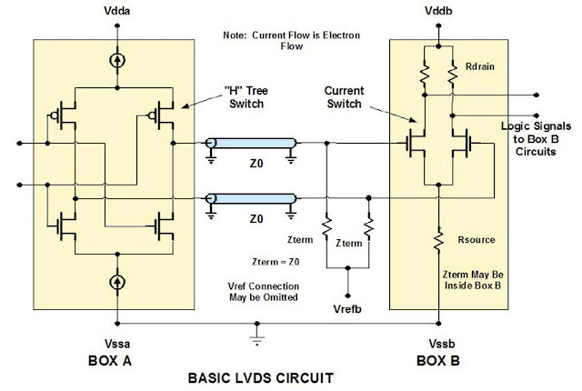
Any electronic product consists of various modules, where each module has to communicate with the other for its operation or to report the status. With the ever-growing demand for faster processing speeds, better response time and more throughputs, always narrow down to highspeed circuits. If not contained properly, the signal flowing t h r o u g h these circuits may radiate energy and can cause problems in the operation of devices in the near vicinity. Now, engineers must consider not only the actual logic on the PCB, but also several other aspects that affect the circuit, including power consumption, PCB size, environment noise, andEMC. The following 10 key EMC design considerations can serve as guidelines and describe how hardware engineers can address EMC issues during the PCB design phase for a system free of EMC faults: 1. Ground Planes : A low-inductance ground system is the most vital element when designing a PCB for minimizing EMI. Maximizing the ground area on a PCB re

FLEX & RIGID-FLEX CIRCUITS

Image
Flex & Rigid-Flex circuits can be shaped to fit where no other design can. They are a hybrid of ordinary printed circuit boards and round wire, exhibiting benefits of each.   In essence, flexible circuits give you unlimited freedom of packaging geometry while retaining the precision density and repeatability of printed circuits. As a high reliability replacement for wire and wire harness assemblies, flex circuits provide a significant cost savings with no reduction in performance. There are a variety of terminations for flex circuits and we can provide all of these as standard manufacturing process. Adding connectors and other minor component assembly is a common practice when producing flex and rigid flex circuits. ·              TYPES OF FLEX CIRCUITS Below you will find information regarding the different types of flexible circuits from a single or double sided design to multi-layer technologies, including rigid flex circuit design specifications. Si