Posts

Showing posts from January, 2016

FLEX & RIGID-FLEX CIRCUITS

Image
Flex & Rigid-Flex circuits can be shaped to fit where no other design can. They are a hybrid of ordinary printed circuit boards and round wire, exhibiting benefits of each.   In essence, flexible circuits give you unlimited freedom of packaging geometry while retaining the precision density and repeatability of printed circuits. As a high reliability replacement for wire and wire harness assemblies, flex circuits provide a significant cost savings with no reduction in performance. There are a variety of terminations for flex circuits and we can provide all of these as standard manufacturing process. Adding connectors and other minor component assembly is a common practice when producing flex and rigid flex circuits. ·              TYPES OF FLEX CIRCUITS Below you will find information regarding the different types of flexible circuits from a single or double sided design to multi-layer technologies, including rigid flex circ...
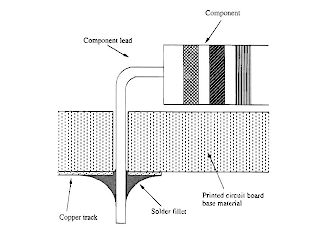
Difference Between Plated through Hole and Non Plated Through Hole

Image
During  PCB design  many issues come across and one of them is in the regard of non-plated and plated through holes. What is the difference between them and where should one use which one? is a commonly asked question. Here we will briefly discuss this issue.  Through hole components  have leads(straight or clinched) and these leads are put through holes available or made on the PCB insulating materials and soldered on the other side onto the copper tracks. The  difference between non plated through hole and plated through hole  is the presence of plated copper inside the insulating base material as shown in the pictures below. The presence of this plated through hole has in turn effect on electrical properties and mechanical stability. When component leads is soldered through plated holes then (1)the electrical resistance by the joint formed becomes less and (2) the mechanical stability increases. This is not the case with the non plated holes and hence p...

placement of connectors and groundings to reduce EMI

Cables and Connectors (1) Cables should be grouped according to their function such as power, analog, digital, and RF. (2) Separate connector assemblies should be used for analog and digital signals. (3) Analog and digital connectors should be located as far apart as possible. (4) Analog and digital signal pins should be separated by unused grounded pins when sharing the same I/O connector. (5) Individual pins should be used inside the I/O connector for each signal return so that all return circuits remain separated. (6) Connector crosstalk may be reduced by using separate power and ground pins for each signal and by reducing the circuit’s loading and current flow.   (7) Cable shields should be grounded to equipment housing at the I/O points. (8) Shielded I/O cables are most effective if grounded at both ends. (9) Cable common mode currents should be removed at the equipment’s metal housing prior to internal connections. (10) Cables shou...

Printed Circuit Board Design Guidelines

Printed Circuit Board Design Guidelines  Below is a list of 16 EMC design guidelines for printed circuit boards along with a short justification for each. 1. The lengths of traces carrying high-speed digital signals or clocks should be minimized. High-speed digital signals and clocks are often the strongest noise sources. The longer these traces are, the more opportunities there will be to couple energy away from these traces. Remember also, that loop area is generally more important than trace length. Make sure that there is a good high-frequency current return path very near each trace. 2. The lengths of traces attached directly to connectors (I/O traces) should be minimized. Traces attached directly to connectors are likely paths for energy to be coupled on or off the board. 3. Signals with high-frequency content should not be routed beneath components used for board I/O . Traces routed under a component can capacitively or inductively couple energy to that compo...

Capacitor Parasitics - Designing for EMI

During your PCB design, an important thing to consider is placement of decoupling capacitors on your PCB for EMI. Capacitors do many things. They filter voltage droops, they present a 'brick wall' for transients, and they try their best to kill any EMI noise on your power rails. One of the most common functions though, is this filtering of EMI noise going into and coming out of the chip on your PCB design. It's supposed to be attached as close as possible to the input power pin of your part with the shortest, fattest trace possible, but surely you're already aware of this (it's also supposed to have the shortest current loop possible between the chip and part, but that's beyond the scope of this article).   For the sake of explanation, you can think of a capacitor as really a capacitor in line with an inductor. Crazy? Yes it is, but it's also unavoidable. If you found a wire lying on the ground and pick it up, it is inherently an inductor of some val...