Posts
Overview of Capacitor technology
- Get link
- X
- Other Apps

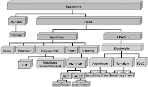
Capacitors (and inductors) have the ability to store electrical energy, inductors store energy as a magnetic field around the component, but the capacitor stores electrical energy directly, as an ELECTROSTATIC FIELD created between two metal "plates". Basic Circuit symbols for capacitors • High Voltage Electrolytic- used in power supplies. • Axial Electrolytic; lower voltage smaller size for general purpose where large capacitance values are needed. • High Voltage disk ceramic; small size and capacitance value, excellent tolerance characteristics. • Metalised Polypropylene; small size for values up to around 2µF good reliability. • Sub miniature Multi layer ceramic chip (surface mount) capacitor. Relatively high capacitance for size achieved by multiple layers, effectively several capacitors in parallel. Uses of Capacitors. Decoupling --The most prevalent use of capacitors ...
Interactive Placement and routing stratagies
- Get link
- X
- Other Apps

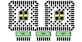
PCB layout is a means to combine your artistic side and your creative skills with the power of automation. I always say that if a PCB design looks good, it will probably work well. However, neatness in routing often leads to unwanted crosstalk as trace segments are routed in parallel for long distances. Interactive Placement - To obtain a high route-completion rate, component placement is extremely important. If the board is difficult to route, it may just be the result of poor placement, slots/gates positioned all over the board, or perhaps the sequence of pins on components are flipped. We need to help the router as much as possible by opening route channels and providing space for vias. Interactive placement is best done by cross-probing and dragging the components one-by-one from the schematic to place on the PCB—taking functionality and design constraints into account. During placement, consideration should not only be given to routing, but also...
EMC design considerations
- Get link
- X
- Other Apps

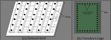
Any electronic product consists of various modules, where each module has to communicate with the other for its operation or to report the status. With the ever-growing demand for faster processing speeds, better response time and more throughputs, always narrow down to highspeed circuits. If not contained properly, the signal flowing t h r o u g h these circuits may radiate energy and can cause problems in the operation of devices in the near vicinity. Now, engineers must consider not only the actual logic on the PCB, but also several other aspects that affect the circuit, including power consumption, PCB size, environment noise, andEMC. The following 10 key EMC design considerations can serve as guidelines and describe how hardware engineers can address EMC issues during the PCB design phase for a system free of EMC faults: 1. Ground Planes : A low-inductance ground system is the most vital element when designing a PCB for minimizing EMI. Maximizing the ground area on a PCB re...
FLEX & RIGID-FLEX CIRCUITS
- Get link
- X
- Other Apps
Flex & Rigid-Flex circuits can be shaped to fit where no other design can. They are a hybrid of ordinary printed circuit boards and round wire, exhibiting benefits of each. In essence, flexible circuits give you unlimited freedom of packaging geometry while retaining the precision density and repeatability of printed circuits. As a high reliability replacement for wire and wire harness assemblies, flex circuits provide a significant cost savings with no reduction in performance. There are a variety of terminations for flex circuits and we can provide all of these as standard manufacturing process. Adding connectors and other minor component assembly is a common practice when producing flex and rigid flex circuits. · TYPES OF FLEX CIRCUITS Below you will find information regarding the different types of flexible circuits from a single or double sided design to multi-layer technologies, including rigid flex circ...
Difference Between Plated through Hole and Non Plated Through Hole
- Get link
- X
- Other Apps

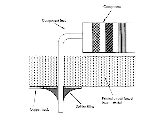
During PCB design many issues come across and one of them is in the regard of non-plated and plated through holes. What is the difference between them and where should one use which one? is a commonly asked question. Here we will briefly discuss this issue. Through hole components have leads(straight or clinched) and these leads are put through holes available or made on the PCB insulating materials and soldered on the other side onto the copper tracks. The difference between non plated through hole and plated through hole is the presence of plated copper inside the insulating base material as shown in the pictures below. The presence of this plated through hole has in turn effect on electrical properties and mechanical stability. When component leads is soldered through plated holes then (1)the electrical resistance by the joint formed becomes less and (2) the mechanical stability increases. This is not the case with the non plated holes and hence p...
placement of connectors and groundings to reduce EMI
- Get link
- X
- Other Apps
Cables and Connectors (1) Cables should be grouped according to their function such as power, analog, digital, and RF. (2) Separate connector assemblies should be used for analog and digital signals. (3) Analog and digital connectors should be located as far apart as possible. (4) Analog and digital signal pins should be separated by unused grounded pins when sharing the same I/O connector. (5) Individual pins should be used inside the I/O connector for each signal return so that all return circuits remain separated. (6) Connector crosstalk may be reduced by using separate power and ground pins for each signal and by reducing the circuit’s loading and current flow. (7) Cable shields should be grounded to equipment housing at the I/O points. (8) Shielded I/O cables are most effective if grounded at both ends. (9) Cable common mode currents should be removed at the equipment’s metal housing prior to internal connections. (10) Cables shou...