Interactive Placement and routing stratagies
PCB layout is a means to
combine your artistic side and your creative skills with the power of
automation. I always say that if a PCB design looks good, it will probably work
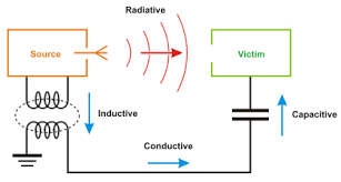
well. However, neatness in routing often leads to unwanted crosstalk as trace
segments are routed in parallel for long distances.
Interactive Placement - To obtain
a high route-completion rate, component placement is extremely important. If
the board is difficult to route, it may just be the result of poor placement,
slots/gates positioned all over the board, or perhaps the sequence of pins on
components are flipped. We need to help the router as much as possible by
opening route channels and providing space for vias.
Interactive placement is
best done by cross-probing and dragging the components one-by-one from the
schematic to place on the PCB—taking functionality and design constraints into
account.
During placement, consideration should not only be given to routing,
but also to inspection and rework. An 80 mil minimum clearance is required for
rework tools, and an angle of 60 degrees for visual inspection. However, where
possible, 45 degrees (i.e., spacing between components = height of tallest
component) is a good rule of thumb.
In other words, if a tall electrolytic
capacitor is next to a BGA, then the height of the electrolytic is the distance
required between components. Along these lines, grouping large, plated,
through-hole components together saves board space.
Similar types of components
should be aligned on the board in the same orientation for ease of component
placement, identification, inspection, and testing. A placement grid of 100
mils is recommended for large components and 25 mils for chip components. Also,
similar component types should be grouped together whenever possible, with the
net list or connectivity and circuit performance requirements ultimately
driving the placements. In memory boards, for example, all of the memory chips
are placed in a clearly defined matrix with pin 1 orientation in the same
direction for all components. This is a good design practice to carry out on
logic designs where there are many similar component types with different logic
functions in each package.
On the other hand, analog designs often require a
large variety of component types, making it understandably difficult to group
similar components together. Regardless of whether the design involves memory,
general logic, or analog components, it’s advisable to orient pin 1 on all IC
components the same, provided that product performance or function is not
compromised in the process.
One issue that is always a problem—especially as
trace widths and clearance decrease— is the lack of via space. With high-speed
design, traces from a BGA fan-out straight to an internal layer to prevent
radiation, and this of course requires a via for each BGA ball. This cannot be
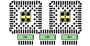
avoided. But we can open up space for
vias on other surface mount devices (SMDs) when using double-sided placement.
Figure Illustrates two PLCCs placed on the top of a board with resistor packs
on the bottom side. If the lands on the bottom are aligned with the lands on
the top, space is cleared for vias and horizontal routing channels are opened.
This is not the case when using blind vias, but certainly helps with
through-board vias.
A comment regarding autoplacement: One of the most useless
features that all EDA layout tools offer is autoplacement. I guess they all
have this feature because some bright guy decided to include this in his tools
and it then became a checkbox for product comparisons—so everyone has to have
it. Notwithstanding the uselessness for autoplacement’s intended purpose, I
have found a good use for it—to see if all the components will fit inside the
board outline before stating placement. If not, then you can re-evaluate the
packaging or reduce functionality to fit the required space.
Cross-probing- Cross-probing, between the schematic and PCB,
provides a valuable mechanism for design, review, verification and testing of
PCBs, but it is most powerful during interactive placement and routing.
Cross-probing is bi-directional, in that you can select parts or nets on the schematic
and highlight and identify them on the PCB database, or vice-versa. This
feature also gives you the ability to drive the router directly from the
schematic design.
Figure above illustrates a schematic to PCB cross-probe of a
component. Cross-probing can also be used as a powerful search tool—locating
parts and nets on the schematic or PCB. And, cross-probing is not limited to
schematic and PCB. AutoVue, for instance, allows the cross-probing between PCB
and 3D MCAD tools, enhancing mechanical visualization of the product.
When an
engineer creates the schematic he invokes a logical process, typically,
grouping components into blocks or sheets that functionally go together. When
the PCB designer then places these components, he should also use a logical, sequential
process by placing functional components near each other, optimizing trace
cross-overs and lengths, keeping constraints in mind.
In years past, I recall
having to place components by select list. This seemed logical but the PCB
designer was never to know whether they were placing a trivial static pull-up
resistor or a critical terminator. Resistors are just resistors—unless you know
what they do. This is the beauty of cross-probing. The functionality of the
circuit is displayed and each and every component can be placed by
functionality and importance—providing error-free transfer of the intended
schematic functionality to the design.
Of course, design rules can also be
added to the schematic to pass this information on to the PCB designer, but a picture
is worth a thousand words.
Interactive Routing- Proper component placement is an
important aspect of routing. If the board is difficult to route, it may just be
the result of poor placement. So before you start routing, it is important to
check the placement and design rules to ensure that there are no issues that
may prevent the route completion. The easiest way to check this is to turn the
autorouter loose and see how it goes. If you do not get at least 85% completion
on this first test route, then you may need to tweak the placement, look at
more appropriate packaging, adjust the design rules, and possibly drop some
functionality to improve routability.
However, there are some important things to do before you
commence with the process of formally routing the board:
1. The stackup should be planned to ensure that controlled
impedance signals have been calculated correctly and that the return current
for each signal layer has a clear return path. The ICD Stackup Planner can be
used to analyze the stackup (download from www. icd.com.au), and help you with
material selection, along with input from your fabricator. The resulting
stackup configuration should then be transferred to the design rules to define
the correct trace width and clearance for each layer, and to specify the
differential pairs.
2. The power distribution network (PDN) should be planned,
and bypass and decoupling capacitors placed in the appropriate positions. The
ICD PDN Planner is an ideal sandbox for analyzing this. It is a good idea to
color the power nets with individual colors so that they can easily be
recognized without having to name the net. Altium has a great feature, which
displays the net name for each net, making identification of power nets
extremely clear.
3. Design rules and
constraints can be passed from the schematic, which automatically sets the
design rules in the PCB database— though there is always some adjustment to be
done on the PCB side. Via sizes for different net classes need to be defined.
This is important for route completion. (Please see my previous article on PCB
Design Techniques for DDR, DDR2 & DDR3, Part 1 and Part 2 for a complete
list of the appropriate design rules for DDR2 routing.) For rules to properly support the design
process, they need to be defined in the correct priority so that the most
important rules prevail over rules of lesser importance.
4. Set up the routing
options. It amazes me that all the EDA tools that I have used do not come with
the router set to the most useful functions straight out of the box. So before routing,
one must tweak the route options to get the tool to do what you want. Details
vary by tool, of course, but the nuisance is near- universal.
Once we have the above set, then it is time to start
interactive routing. The real power of cross-probing is driving the router from
the schematic. Starting with the most critical nets, cross-probe in the
following sequence:
1. Select the components on the schematic and fan-out on the
PCB selecting the appropriate pattern. Adjust the fan-out as necessary. The
rules should be set such that power traces are routed thick (10 - 20 mils) to
reduce inductance. And, each GND and VCC should have its own individual via to
the plane—avoid connecting two or more GNDs to the one via.
2. Obviously, matched length, differential pair and critical
signals that have specific requirements should be routed first. Fix or lock
these traces so they cannot be inadvertently moved.
3. Select the most
critical nets, a few at a time, on the schematic and route in the PCB. Adjust
the routing as necessary then move on to the next group of nets and so on. In
this way you can build up an excellent route in a short time and it is all
controlled from the schematic. Feel free to jump in and tweak the routing to
your liking.
Once the routing is complete, apart from running design rule
checks (DRCs), I like to run a sanity check on the board. I can either do this
in the simulation environment or in the PCB database. Simply highlight each net
one by one—it is tedious, but gets results. You can quickly see if there are
any nets that are longer than the Manhattan length or spiral around the board
three times before termination.
Hope it will helpful for Readers...
Happy Reading...


Comments
Post a Comment