Posts

Decoupling, Bypassing and Filtering

Decoupling, Bypassing and Filtering ( 1) EMI filters can be used as a shunt element to divert electrical currents from a trace or conductor; as a series element to block a trace or conductor current; or they may be used as a combination of these functions.    Selection of the filter elements should always be based on the desired frequency range and component characteristics.    A low pass filter can be useful for reducing most high frequency EMI problems.    It incorporates a capacitive shunt and series resistance or inductance.    However, at frequency extremes, the capacitor can become inductive and the inductor can become capacitive causing the filter to act more like a band-stop filter.     The filter design type should be based on the overall impedance at the circuit’s point of application for proper match.    A T-filter design is effective for most EMI applications and is ideal for analog and digital I/O ports....
Tips for Electronic Printed circuit Board Design

EMI/EMC problems may be approached at the component, PC board or enclosure levels.    However, it is much more efficient to deal with these problems as close to the source or susceptible victim as possible.    Therefore, it is important to consider these tips as guidelines for PCB design and layout so that problems may be identified and prevented prior to actual fabrication of the equipment. (1) EMI controls should be applied at the circuit and box levels prior to addressing EMI at the interconnected and system levels. (2) Digital circuits are more likely to be the source of emissions due to the handling of periodic waveforms and the fast clock/switching rates.    Analog circuits are more likely to be the susceptible victims due to higher gain functions. (3) The source or susceptible victim of most EMI problems is typically an electronic component .    Although active components are usually the sources of EMI , passive components ...

Identifying Potential EMI Sources and Victims

Image
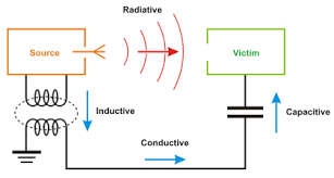
As mentioned in my previous Article i am trying to elaborate the EMI source and victims. After seeing the word EMI you must be thinking  what is it? Below is the small definition of EMI. Electromagnetic Interference (EMI) The process where disruptive electromagnetic energy is transmitted from one electronic device to another via radiated or conducted paths. –  Radiated Emissions -The component of RF (roughly 10kHz to 100GHz) energy transmitted through a medium, usually free space (air), as an electromagnetic field. –  Conducted Emissions -The component of RF energy transmitted as a propagating wave generally through a wire or interconnect cable. LCI (Line conducted interference) refers to RF energy in the power cord.   A typical circuit board may have dozens, hundreds or even thousands of circuits. Each circuit is a potential source of energy that might eventually be coupled unintentionally to other circuits or devices. Each circuit is also a poten...

Strategies for Laying Out Printed Circuit Boards.

Image
Most board designers employ a list of guidelines to help place components and route traces. For example, a typical guideline might be "minimize the length of all traces carrying a digital clock signal." Often, a designer is not familiar with the reason for the guideline or does not fully understand the consequences of violating the guideline for a particular application. Quiz Question Suppose you're laying out a high-speed multi-layer printed circuit board and you need to route a trace carrying a high-frequency signal from a digital component to an analog amplifier. You want to minimize the chance of having an electromagnetic compatibility (EMC) problem, so you search the web for EMC design guidelines and you find three guidelines that seem to pertain to your situation: 1.         minimize the length of high-speed traces; 2.         always gap any solid planes between analog and digital circuits; and 3.  ...

Do's and Don'ts for PCB Layer Stack-up

Image
Each day the electronic gadgets complexity increases with the miniaturization requirements, boards are becoming much denser. Multilayer PCB technology can satisfy today’s miniaturization board requirement. Multilayer PCBs has more than two layers of PCBs, arrangement of layer should be done with great care because inefficient layer arrangement will lead to the noisy board with unexpected performances. This article addresses the layer stack-up basics and the general layer stack-up considerations. 2 . Layer stack-up basics  Layer stack-up specifies the proper arrangement of circuit board layers for multilayer boards before starting board layout design.  Stack-up mainly defines which layers should be solid power and ground planes, the substrate (dielectric constant), and the spacing between layers.  While planning a layer stack-up, also compute the desired trace dimension and minimum trace spacing. SIDE VIEW    Multilayer boards ...

Difference between through hole and Surface mount components

Image
As technology grows the demand for less weight and smaller size component increases. This leads to new improved technology known as   surface mount technology   (SMT). Surface mount components are similar to plated through hole as far as there electrical function is concerned but the key difference is in their size. The small size of surface mount components (SMC) provides better electrical performance. Surface mount components are placed or mount directly on Printed circuit board (PCB) which means they do not require hole for mounting the component. They can be directly soldered on track side. Surface mount components have different shape leads and they have little circular at bottom etc for soldering as shown in figure below. SMD devices are mainly found in multi-layer PCB where size of device is major concern. They can also be used on boards or devices which contain both through hole and SMC because some components like transformer, heat sink are not suitable...