What is a differential pair and how does it work?
In its most basic form, a differential pair is made up of two transmission lines that have equal and opposite polarity signals travelling on them. The property that these two signals have in common is that they are equal and opposite and they are tightly timed to each other.
Beyond these two characteristics there are no other properties that matter when a design uses differential pairs. Maintaining the equal and opposite amplitude and timing relationship is the guiding concept when using differential pairs.
figure 1
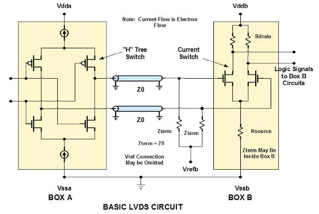
Figure 1 is a typical CMOS differential pair driver and receiver pair. It is the usual circuit used in LVDS (low voltage differential signaling) type signaling protocols.
figure 2
As can be seen from Figure 1, there are two independent transmission lines of characteristic impedance, Z0, connecting the drivers and receivers. Each of these is terminated with a parallel termination of value Z0 to Vref in or at the receiver. Figure 2 shows the current flow in the two signal paths when the circuit is in one of its two logic states. In the other logic state the current reverse direction. (The two lines do not have to be the same impedance for the circuit to function properly).
As can be seen, the current flows out of the current source in Box A through the upper transmission line and into Vrefb. A different current flows out of Vrefb, up through a terminating resistor, through the lower transmission line and into the upper current source. When all of the impedances in the path are of equal magnitude,the two currents are equal and opposite flowing into and out of Vrefb so the net current into or out of Vrefb is zero. When this is the case,it is convenient to leave off the Vrefb connection and place a single resistor of 2 times Z0 across
the two ends of the pair. When the impedance of the two lines is 50 ohms each, this results in a single resistor of 100 ohms. As a result, those who don’t understand how this circuit works mistakenly conclude that a 100-ohm differential impedance is required, when, in fact, what
is needed is two 50-ohm transmission lines each terminated in 50 ohms.
The receiver responds only to the difference in voltage between the ends of the two transmission lines and makes a decision as to whether a “1” or a “0” is present. When the polarity reverses, a logic state change is detected and sent on to circuits in the receiver box. It is at the
moment of crossing that the logic state change is sensed. It is for this reason that minimizing jitter is so important. The receiver is a crossing detector so preserving the integrity of the crossing is essential. It is the primary concern when designing a differential pair.


Comments
Post a Comment