Do's and Don'ts for PCB Layer Stack-up
Each day the electronic gadgets complexity increases with the miniaturization requirements, boards are becoming much denser. Multilayer PCB technology can satisfy today’s miniaturization board requirement. Multilayer PCBs has more than two layers of PCBs, arrangement of layer should be done with great care because inefficient layer arrangement will lead to the noisy board with unexpected performances. This article addresses the layer stack-up basics and the general layer stack-up considerations.
2. Layer stack-up basics
Layer stack-up specifies the proper arrangement of circuit board layers for multilayer boards before starting board layout design. Stack-up mainly defines which layers should be solid power and ground planes, the substrate (dielectric constant), and the spacing between layers. While planning a layer stack-up, also compute the desired trace dimension and minimum trace spacing.


 SIDE VIEW
Multilayer boards are made up of one or more cores and prepreg as shown in figure . Cores are made up of a copper-plated glass-reinforced epoxy laminate sheets. Figure shows a core can have copper on one or both sides. Cores are glued together with sheets of a partially cured epoxy. This sheets are referred to as prepreg as shown in figure .
Below points set out some basic do’s and don’ts points for planning layer stack-up.
Things to do..
1.To reduce the layer stack-up planning complexity and time, first plan the power and ground layers. To plan a power and ground layers, first establish the signal rise times, the number of signals, and the physical dimensions of circuit board. As the trace width assumption is not particularly critical at this stage, make a guess for the trace width. Determining the best trace width for board is matter of experience and guesswork
» As ground planes diminish the electromagnetic interference and electromagnetic radiation by absorbing high frequency noises, plan ground plane on the outer sides of the board. It is good practice to have ground plane on either one-side or both-side of board.
» Noise and crosstalk generation due to inductance and capacitance may generate crisis, so next estimate the mutual-inductance, mutual-capacitance by building desired models of solid power, split power, hatched, and solid ground plane. This model will give the complete idea of actual current directions, which help to provide stable voltage references, too. Generally split power planes should use to provide proper isolated areas on a power plane layer while providing an electrically different reference point (analog and digital sources).
» In high speed circuit board use solid ground and solid power plane in pair that gives best capacitive coupling to reduce power supply noises. » Sometimes to reduce the return current path, power planes can be used as low-inductance signal return-current paths just as ground plane.
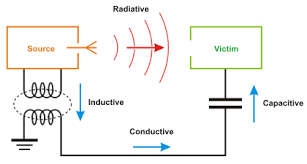
» For external interfaces (Ethernet, PCIe, USB, etc.), high speed signals need to drag outside boards. If the ground for that high speed interface is connected to ordinary digital ground, the effective interface output may be affected by a noise voltage presented on the digital logic ground.
» As the digital logic grounds are notorious for high speed noise voltages which can exceed FCC limits, one effective solution to this problem is to add an extra chassis ground plane to the same layer as shown in figure 3. Some below mentioned rules of thumb should be followed for planning chassis ground planes

» Chassis ground plane should stack directly next to a ground plane, giving a very tight capacitive coupling between the two planes. Then chassis ground plane should screw, solder, or weld to external chassis to the earth.
» For only high frequency noises, chassis ground plane is effectively shorted to the digital ground via high voltage capacitor with low ESR. This bypass capacitor also provides best ESD protection.
» With the chassis ground plane approach, the digital and external chassis remain electrically isolated at low frequencies for desirable for safety proposes. » In case of isolation is not mandatory, simply short digital logic ground directly the chassis without using a separate chassis ground layer.
» With more layers, board size can spread out farther. That makes routing easier and reduces the risk of crosstalk problems. Unfortunately, PCB cost is proportional to the number of layers and the board surface area. So design should have fewest numbers of layers.
» Forcing traces tightly together increases the circuit board density. Vary dense designs required fewer circuit board layers.
» Smaller, more closely spaced traces also can produce more crosstalk and less power handling capacity. So plan traces width and pitch according to amount of current flowing through it and type of signal. This tradeoff among crosstalk, routing density, and power capacity is critical to low-cost production device.
» Use 0.5 oz. copper thickness for outer side layers, and use 1 oz. thickness for inner side layers to provide better current handling capacity with drastic temperature rise.
» High speed plane, used to design striplines or microstrips can buried between power or ground plane layers for extra shielding as show in figure 2.
» The purpose of solder mask layer is to physically and electrically insulate those circuits to which no soldering is required. Solder mask can reduce a little impedance on thin traces. But as the trace thickness increases solder mask has less affect. So the effect of the solder mask should be considered during impedance calculation.
» Much of the board manufacturers are following commercial standards that are published by the IPC organization for board manufacturing, assembly, and quality control. So IPC standard adoption for board dimensions, board thickness, core thickness, copper cladding thickness, Prepreg thickness, solder mask tolerance can reduce the production time and cost, increases the product reliability.
Things not to Do
» Do not design odd number of layers in stack-up. Odd layers boards can be manufactured, but it is usually simpler and less expensive to manufacture boards with an even number of layers. It is recommended to add an extra ground layer rather than designing odd layer boards.
» Do not split the ground plane into separate planes for analog, digital, power pins. A single and contiguous ground plane is recommended.
» Do not overlap two different high speed signals on two different layers; the capacitive coupling should be minimum to reduce the crosstalk across them. It is recommended to reduce overlap area by planning adjacent horizontal and vertical planes as show in figure 2.
» Do not overlap power supply layer and digital high speed signal layer. It is recommended to prepare layer partition map after components placement.
» Do not leave void spaces in layer, it is recommended to pour void spaces by copper. And short pour copper to ground plane by printed through hole which reduces the electromagnetic interference and the crosstalk.
» Do not use ordinary capacitors as a bypass capacitor between chassis ground and digital ground, because they might have too much lead inductance and also high ESR. Use only the high voltage capacitors with low ESR and low temperature coefficient as a bypass capacitor.
This Article outlines numerous points that must be carefully reviewed and while determining the stack-up, try to achieve below points.
1. Manufacturing limitation needs to be check with respect to maximum number of layer, minimum trace width, and minimum drill size, aspect ratio of the board, PCB material thickness and type.
2. Signal layer should have at least one adjacent plane without any split.
3. Power and ground layer should be adjacent to each other.
4. High speed signal layer should be sandwich between two ground layer which provides shielding effect.
5. Power plane can also work as return plane for the high speed signal routing.
Hopefully this will help the Readers..
Thanks,
Ruby

The pictures are quite impressive as they show all the solutions for the pack-ups of these multilayered PCB’s which are common in use now.
ReplyDelete