Popular posts from this blog
Do's and Don'ts for PCB Layer Stack-up
Each day the electronic gadgets complexity increases with the miniaturization requirements, boards are becoming much denser. Multilayer PCB technology can satisfy today’s miniaturization board requirement. Multilayer PCBs has more than two layers of PCBs, arrangement of layer should be done with great care because inefficient layer arrangement will lead to the noisy board with unexpected performances. This article addresses the layer stack-up basics and the general layer stack-up considerations. 2 . Layer stack-up basics Layer stack-up specifies the proper arrangement of circuit board layers for multilayer boards before starting board layout design. Stack-up mainly defines which layers should be solid power and ground planes, the substrate (dielectric constant), and the spacing between layers. While planning a layer stack-up, also compute the desired trace dimension and minimum trace spacing. SIDE VIEW Multilayer boards ...
Identifying Potential EMI Sources and Victims
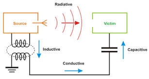
As mentioned in my previous Article i am trying to elaborate the EMI source and victims. After seeing the word EMI you must be thinking what is it? Below is the small definition of EMI. Electromagnetic Interference (EMI) The process where disruptive electromagnetic energy is transmitted from one electronic device to another via radiated or conducted paths. – Radiated Emissions -The component of RF (roughly 10kHz to 100GHz) energy transmitted through a medium, usually free space (air), as an electromagnetic field. – Conducted Emissions -The component of RF energy transmitted as a propagating wave generally through a wire or interconnect cable. LCI (Line conducted interference) refers to RF energy in the power cord. A typical circuit board may have dozens, hundreds or even thousands of circuits. Each circuit is a potential source of energy that might eventually be coupled unintentionally to other circuits or devices. Each circuit is also a poten...


Nice blog regarding PCB design service. Day by day, there are many new and the
ReplyDeletequality circuit board is manufactured using advance technology.Few month ago I had contacted a company OM ELECTRONICS for my PCB requirement through a blog.They have sent me some sample PCB with good quality and my requirement is on processing .
Printed circuit board manufacturers